Physical Methods of Speed-Independent Module Design english
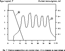
In Section 2 we presented series-parallel model of computations in CL. We showed that in every moment during switching current consumed by CL is a superposition of the currents consumed on the activated signal propagation paths (SPPs). Now, considering CL implemented by CMOS devices we should note that while logical signal propagates through SPP the neighbouring gates switch in opposite directions. That is why a curve of current consumed by a ten inverter chain (Fig.8) looks like a combination of crests and troughs. Nevertheless, in the very lowest point of the curve the current consumed by CL in a transient state remains several orders more than in a steady state.
4.2 OVD implementation
The proposed OVD circuit, shown in Fig.9, is a threshold circuit translating an analog current signal I into a logical signal OV.
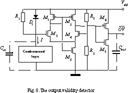
The OVD circuit contains a current-to-voltage converter (CVC) consisting of the resistor R1 and the diode D1. The OVD also contains a comparator implemented by the MOS transistors M1-M7 and resistors R2,,,R3 . CMOS CL consumes the current I and introduces a capacitance Cin . The capacitance Cout represents the load caused by the interface circuitry. A low potential output signal of OVD corresponds to CL output validity. A high potential output signal corresponds to CL output invalidity. So, OVD generates OV signal in negative logic manner.
The transfer characteristics of CVC is determined by a system of three equations:
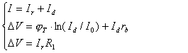
where I is an input current of CVC, DV is a voltage drop on the CVC circuit, Ir is a current flowing through the resistor R1, Id is a current passing through the diode D1, I0 is a leakage current of the diode, rb is a bulk resistance of the diode. Here stands for kT/q where k is Boltzmann's constant, T is absolute temperature, q is charge of an electron.
Equations (1)-(3) determine the functional connection F between input current I and voltage drop DV: . Graphic solution of the system is shown in Fig.10.

CVC parameters to be calculated are R1 and rb. Initial data for calculating R1 are the threshold voltage drop DVth and corresponding threshold input current Ith . Value Ith is determined by minimal current consumed by CMOS CL in transient state. Initial data for calculating rb are maximal voltage drop DVmax and corresponding maximal input current Imax. Value Imax is determined by the maximal number of gates in CL switching simultaneously and their load capacitances.
The comparator chosen is the CMOS ECL receiver proposed by Chappell et al.[11]. The circuit includes a single differential amplifier stage with built-in compensation for parameter variations, followed by a CMOS inverter. The comparator has 100-mV worst-case sensitivity in 1-mm technology. Detailed static and dynamic analysis of the comparator circuit was given in [11].
The comparator compares input voltage signal Vin with reference voltage Vref. If Vin <Vref the comparator output signal equals to logical zero which means that CL outputs are valid. Otherwise, Vin >Vref, the comparator output signal equals to logical "one" which means that the outputs are invalid.
As it follows from the OVD circuit configuration,
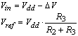
where Vdd is a voltage of power supply.
Equations (4) and (5) allow us to calculate the threshold voltage drop DV of the CVC circuit:
since 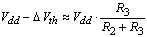 , so
If 0<DV<500mV then the diode D1 of CVC operates in the very small current region Id » 0 and Id <<Ir. So the component Id in the Equation (1) can be neglected and I»Ir =DV/R1 .
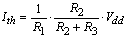
For practical values of  the threshold input current of the OVD circuit is reversely proportional
to the resistance of R1 :
 . Substituting Equation (6) yields
 .
As to choosing value of rb it must be done with regard to maximal voltage drop DVmax .
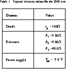
If DV>750mV, the diode D1 is in active mode and while rb <<R1 the condition Ir <<Id is true. So, in the large current region I»Id and Equation (2) determines an almost linear dependence between I and DV. For instance, if the maximal voltage drop DVmax =900mV and maximal input current Imax=2mA, then in accordance with the Equation (2) rb »100W. Typical element values for the OVD circuit with DVth =400mV are given in Table 1.
The turn-on ton and turn-off toff delays of the OVD circuit depend on the OVD itself and the CMOS CL as well. (Switching the OVD output from low to high voltage is called "turning-on" and reverse switching is called "turning-off".)
Consider a piece of CMOS CL and its interaction with OVD circuit (Fig.11). The piece is an SPP including N logic gates. Each gate is shown symbolically as a connection of PMOS and NMOS networks. All the capacitances affecting ton and toff can be brought down to three components:
(i) CLi is the load capacitance of the i-th gate;
(ii) Cpsi is the power supply bus capacitance associated with the i-th gate;
(iii) Cin is the input capacitance of the OVD circuit.
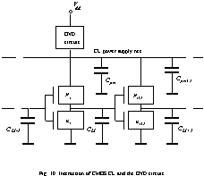
Let pi is a probability of the i-th gate being in the state of high output potential. In this state the capacitance CLi is connected with power supply bus through the low channel resistance of turned-on transistors in PMOS network of the i-th gate. Then equivalent capacitance Ceq connected to the OVD circuit input equals
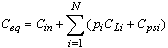 (7)
where N is a number of gates in the considered SPP. Here the resistance of conducting PMOS network is assumed to be negligible.
Equation (7) is also true for CL including several SPPs. In that case summing must be carried out for all the gates belonging to CL.
Simulation shows that ton and toff are proportional to the OVD time constant t=R1Ceq. It was also obtained that when N>20, the component under the sign of summation in Equation (7) can be much larger than the component Cin. Due to voltage drop DV the effective power supply voltage is reduced and CL performance is decreased by about 35 percent [7].
In order to make SIM operating faster special attention must be paid to reducing the capacitance introduced by CL.
4.3 Speed-independent address bus
The simplest case of CL is a scheme degenerated into a set of wires called a multi-bit bus. Let us develop the OVD circuit for such a CL.
Multi-bit bus consists of several lines. Each line can be considered as a medium for signal propagating from one end of the chip to another. Delay of signal propagation through a line depends on several factors:
(a) output impedance and symmetry of driver circuit;
(b) initial state of the line: if driver is symmetrical, line switching from high to low voltage lasts shorter than reverse switching;
(c) electrical properties of the line as a signal propagation medium (resistance of conducting layer and capacitances between the line and other wires next to it);
(d) length of the line;
(e) input impedance and sensitivity of receiving circuit.
Since different lines of the bus operate in different conditions (a)-(e), signal propagation delays are different, too. From the standpoint of environment the bus behaves like any other more complicated CL.
Asynchronous RAM designers use a bus transition detector since 1980s [13-15]. Such a detector is usually based on double-rail address coding and two series connected transistors for each address bit [15]. One of the transistors receives the true address signal and the other receives the complementary address signal of the particular address bit. For any steady state condition one of the transistors will be turned on and one will be turned off. There will be a finite rise and fall time during a transition of the address bit. There is a short time during which both transistors are conducting. The establishment of the conductive path provides the detection of the address transition. In the first asynchronous RAMs the output signal of the transition detector is used for bit line precharging and for enabling/disabling sense amplifiers and peripheral circuitry.
Self-timed RAM announced in 1983 [14] used transition detectors not for address transition only but also for detecting read/write completion and address/bit line precharge completion as well.
The CMOS transition detector was invented in 1986 [15]. This circuit is also based on double-rail coding and uses a pair of series-connected NMOS transistors (Fig.12). The scheme for n-bit bus control contains n line transition detectors (LTDs) and n AND-gates. Outputs of AND-gates are united in node M forming wired OR. The output inverter serves as a pulse shaper. Capacitors C1 and C2 are intended to prolong rise time of the LTD output signal (true and complementary). This is necessary for reliable detection.
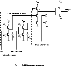
The main drawback of the circuit is speed dependence. One can see that if true and complementary address bit signal have different propagation delays, the conducting path via NMOS transistors will never be formed.
Using the OVD circuit proposed in Section 4.2 as LTD we can avoid this drawback.
Note that address transmission through the address bus is unidirectional. So to detect completion of bus transition it is enough to recognize the bus state at the destination end. For this purpose we modify CL to consist of n lines. The modification means introducing n LTDs, each actually a CMOS inverter chain. Each chain contains two inverters loaded with a capacitance (Fig.13). Input of each LTD is connected with corresponding line of the bus at the destination end. Power supply pads of all LTDs are connected to the current input of the same OVD circuit.
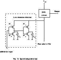
The parameters of the input current signal for the OVD circuit are varied by
(i) value of capacitances C1 and C2 ;
(ii) dimensions of MOS transistors M1 -M4 .
Since all transitions in CL are of the same duration and can be lengthened to be outlast the OVD turning-on time, we simplify the interface circuitry by disallowing the asymmetrical delay.
Due to short duration of normal transition in this CL we must take into account the integral nature of the sensitivity of the OVD circuit. OVD sensitivity depends on both amplitude and width of input current pulse. Simulated operation region of the OVD circuit for current pulses shorter than 30ns is shown in Fig.14. It is obvious that in this case the threshold of the OVD circuit must be determined by threshold charge Qth value. The OVD input charge Q equals to where I is OVD input current, t is a moment of time when transition occurs, w is a width of input current pulse. Turning-on condition for the OVD circuit is Q=Qth.
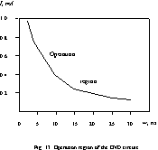
When the LTD circuit shown in Fig.13 is used, the charge value Q is determined by either C1 or C2.
Namely, if the line goes from low to high voltage, Q=dV×C2. If the line goes in
the reverse direction then  where dV is charging/discharging
voltage, approximately equal to the effective power supply voltage: dV»Vdd -DV. Here Vdd
is OVD power supply voltage and DV is CVC voltage drop.
The OVD circuit with typical parameters (See Table 1) has a threshold charge value Qth =4.0×10⁻¹² C. When C1 =C2 =CL , the minimal value of CL providing OVD capacity for operation is about 1.0×10⁻¹² F.
Influence of transistors M1 -M4 dimensions on LTD delay d is determined by approximation [17]:
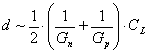
where