Physical Methods of Speed-Independent Module Design english
Since  and where W and L are width and length of transistor channels of the corresponding conduction type, the LTD delay d
is proportional to
 .
It has been obtained that for  , , CL=1.0pF and Vdd-DV=5.0V the LTD delay d=7.6ns.
When LTD works jointly with the OVD in the speed-independent bus, the real value of the LTD delay will increase by 30-40 percent due to OVD's R1 effect on the effective power supply voltage.
To determine the appropriate value of R1 in the OVD circuit we must know threshold input current Ith corresponding to threshold voltage drop DVth recommended to be equal to 400mV.
Average input current Iav in transient state of one line is determined by the expression Iav =CL×v where v is the average rate of increase in the output signal for an inverter included in LTD. For typical values v=1.0×10⁹ Volts per second and CL =1.0pF, Iav =1.0mA. Accepting Ith =0.4mA and Imax=2.0mA we obtain R1=1kW and rb=100W.
Simulation has shown that in this case OVD turning-on delay can be approximated by an empirical expression:
ton[ns]=8.1+0.1×n
where n is the address bus bit capacity. Total delay of recognizing address transition ttot =d×g+ton where g is a coefficient of the LTD delay increase due to reducing power supply voltage. As we showed above g»1.35. It can be seen that if n=32, ttot=21.6ns.
4.4 Speed-independent adder
The circuit we use in this Section as a CL was a touch-stone for many speed-independent circuit designers for about four decades. We mean a ripple carry adder (RCA) which is actually a chain of one-bit full adders (Fig.14).
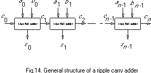
Each full adder calculates two Boolean functions: sum si=aiÅbiÅci and output carry ci+1=aibi+bici+aici where ai, bi are summands, ci is input carry and Å stands for XOR operation.
In 1955 Gilchrist et al. proposed speed-independent RCA with carry completion signal [18]. In 1960s that circuit was carefully analyzed and improved [19-21]. In 1980 Seitz used RCA for illustrating his concept of equipotential region and his approach to self-timed system design [4].
Now we use RCA as a CL for illustrating our approach to SIM design.
As it was shown in Section 4.2 the turn-on and turn-off delays of the OVD circuit are proportional to the equivalent capacitance Ceq associated with OVD circuit input. Capacitance Ceq depends linearly on a number of gates N in CMOS CL. To speed up a SIM it is necessary to reduce a number N. This can be reached by structural decomposition CMOS CL into subcircuits CL1, CL2, etc. Each subcircuit CLi is connected to its own detecting circuit OVDi or directly to the power supply if this subcircuit transition does not affect the transition duration in CL as a whole. Each detecting circuit OVDi generates its own OV signal which is combined with other OVDs' output signals via a multi-input OR (NOR) element. The output signal of that element serves as OV signal of the CMOS CL.
Multi-bit RCA computation time is determined by length of maximal activated carry chain. A lot of papers were devoted to analysis of carry generation and carry propagation in RCA [19-21], many of them contained their own methods for estimation or calculation of average maximal activated carry chain. We do not intend to add another one.
Let us have a look inside RCA. As it was mentioned above RCA consists of one-bit full adders and each full adder consists of two parts: forming sum si part and forming carry ci+1 part (Fig.16).
In multi-bit RCA all forming sum parts do not interact with each other and do not affect on transition duration in RCA. Each forming carry ci+1 part receives ci signal from preceding forming carry part and sends ci+1 signal to consequent one.
To decompose RCA we use three heuristic tricks:
(i) All forming sum parts we connect directly to power supply.
(ii) We divide each forming carry part into three subcircuits denoted in Fig.16 by numbers 1,2 and 3. All subcircuits 1 we connect directly to power supply because they do not contain input ci and so do not contain carry propagation path.
(iii) All subcircuits 2 we connect to OVD1 and all subcircuits 3 we connect to OVD2. Outputs of OVD1 and OVD2 are connected to two-input NOR-gate forming RCA OV signal in positive logic manner (Fig.17).
OVD1 and OVD2 input currents I1 and I2 curves for 6-bit RCA and longest transition duration are shown in Fig.18.
Accepting DVth1,2=400mV we calculated the OVD circuits parameters. It was obtained R11=5kW, Ith1=0.08mA, R12=3kW, Ith2=0.13mA. OVD1 and OVD2 delay dependencies on a number of bits in RCA are shown in Fig.19.
4.5 Comparison of SIMs with synchronous counterparts
Transition duration in CL is a random variable. Probability of transition with duration D is determined by implemented Boolean function and distribution of input logical combinations. Domain of possible values for variable D occupies the interval [0;Dmax]. Here Dmax is a length of critical path in CL.
Let  is a mathematical expectation of transition
duration in CL where Di is a length of i-th SPP in CL, pi is a
probability of i-th path being the longest activated SPP.
When CL works in the synchronous mode, the cycle duration Ts is chosen with regard to maximal transition duration Dmax. Certain margin must be added to Dmax to provide reliable operation of CL in the case of CL parameter variations: Ts =k×Dmax where k is a margin coefficient.
In SIM cycle duration is a random variable with expectation Tsi = g×Dme+toff+tif where g is a coefficient of CL delay increasing due to reducing power supply voltage, toff is turn-off delay of the OVD circuit, tif is an interface circuitry delay.
We determine efficiency E for speed-independent mode of CL operation as relative increase of SIM performance
in comparison to its synchronous counterpart: .
Generally, speed-independent mode is more efficient than synchronous one if Ts >Tsi
or, in other words,  .
In the case of RCA  where tc is a delay of
carry forming part, n is a number of full adders in RCA.
It has been shown [19] that in n-bit RCA Dme» tc×log2(5n/4). Then, in the case of speed-independent operation Tsi=g×tc×log2(5n/4)+toff+tif.
We have obtained dependencies of Ts , Tsi on a number of bits in RCA that are shown in Fig.20. As it can be seen, speed-independent operation of RCA is more efficient while n>8.
5.Conclusion
6.Acknowledgement
I would like to thank Igor Shagurin and Vlad Tsylyov of the Moscow Physical Engineering Institute for helpful discussions of this work. I am also grateful to Chris Jesshope of University of Surrey and Mark Josephs of Oxford University who kindly provided the latest material on their research in the area of delay-insensitive circuit design.
References
[1] Miller, R.E., Switching theory (Wiley, New York, 1965), vol.2, Chapter 10.
[2] Unger, S.H., Asynchronous Sequential Switching Circuits (Wiley, New York, 1969).
[3] Armstrong, D.B., A.D. Friedman, and P.R. Menon, Design of Asynchronous Circuits Assuming Unbounded Gate Delays, IEEE Trans.on Computers C-18 (12) (1969) 1110-1120.
[4] Seitz, C.L., System timing, in: C.A. Mead and L.A. Conway, eds., Introduction to VLSI Systems (Addison-Wesley, New York, 1980), Chapter 7.
[5] Izosimov, O.A., I.I. Shagurin, and V.V. Tsylyov, Physical approach to CMOS module self-timing, Electronics Letters 26 (22) (1990) 1835-1836.
[6] Veendrick, H.J.M., Short-circuit dissipation of static CMOS circuit and its impact on the design of buffer circuits, IEEE J. Solid-State Circuits SC-19 (4) (1984) 468-473.
[7] Chappell, B.A, T.I. Chappell, S.E. Schuster, H.M. Segmuller, J.W. Allan, R.L. Franch, and P.J. Restle, Fast CMOS ECL receivers with 100-mV worst-case sensitivity, IEEE J. Solid-State Circuits SC-23 (1) (1988) 59-67.
[8] Chu, S.T., J. Dikken, C.D. Hartgring, F.J. List, J.G. Raemaekers, S.A. Bell, B. Walsh, and R.H.W. Salters, A 25-ns Low-Power Full-CMOS 1-Mbit (128K´8) SRAM, IEEE J. Solid-State Circuits SC-23 (5) (1988) 1078-1084.
[9] Frank, E.H., and R.F. Sproull, A Self-Timed Static RAM, in: Proc. Third Caltech VLSI Conference (Springer-Verlag, Berlin, 1983) pp.275-285.
[10] Donoghue, W.J., and G.E. Noufer, Circuit for address transition detection, US Patent 4563599, 1986.
[11] Huang, J.S.T., and J.W. Schrankler, Switching characteristics of scaled CMOS circuits at 77K, IEEE Trans. on Electron Devices ED-34 (1) (1987) 101-106.
[12] Gilchrist, B., J.H. Pomerene, and S.Y. Wong, Fast Carry Logic for Digital Computers, IRE Trans. on Electronic Computers EC-4 (4) (1955) 133-136.
[13] Hendrickson, H.C., Fast High-Accuracy Binary Parallel Addition, IRE Trans. on Electronic Computers EC-9 (4) (1960) 465-469.
[14] Majerski, S., and M. Wiweger, NOR-Gate Binary Adder with Carry Completion Detection, IEEE Trans. on Electronic Computers EC-16 (1) (1967) 90-92.
[15] Reitwiesner, G.W., The determination of carry propagation length for binary addition, IRE Trans. on Electronic Computers EC-9 (1) (1960) 35-38.
Appendix
SPICE2G.6: MOSFET model parameters
|
|
VALUE | ||||
| Name | Parameter | Units | PMOS | NMOS | |
|
1 |
level | model index | - |
3 |
3 |
|
2 |
VTO | ZERO-BIAS THRESHOLD VOLTAGE | V |
-1.337 |
1.161 |
|
3 |
KP | TRANSCONDUCTANCE PARAMETER | A/V2 |
2.3×10⁻⁵ |
4.6×10⁻⁵ |
|
4 |
GAMMA | BULK THRESHOLD PARAMETER |

|
0.501 |
0.354 |
|
5 |
PHI | SURFACE POTENTIAL | V |
0.695 |
0.660 |
|
6 |
RD | DRAIN OHMIC RESISTANCE | OHM |
333 |
85 |
|
7 |
RS | SOURCE OHMIC RESISTANCE | OHM |
333 |
85 |
|
8 |
CBD | ZERO-BIAS B-D JUNCTION CAPACITANCE | F |
1.98×10⁻¹⁴ |
6.9×10⁻¹⁵ |
|
9 |
|||||